
세계의 삼성, 20 nm공정으로 NAND형 플래쉬 메모리의 양산 개시 세계 최초

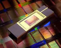
【서울 시사】한국의 삼성 전자는 19일, 회로 선폭 20나노미터(나노는 10억분의 1) 공정으로, 32 기가비트의 NAND형 플래쉬 메모리의 양산을 개시했다고 발표했다.동공정으로의 메모리 반도체의 양산은 세계 최초라고 한다.(2010/04/19-12:22)

미안한 ・・・
그래,
또야 ・・・
프레스 릴리스의 원문을 보았으면 좋겠다.
SAMSUNG Producing Industry’s First Higher-performing 20nm-class NAND Flash Memory
Seoul, Korea on Apr 19, 2010 Seoul,
Korea - April 19, 2010 : Samsung Electronics Co., Ltd., the world
leader in advanced semiconductor technology solutions, today announced
the industry"s first production of 20 nanometer (nm) class NAND
chips for use in Secure Digital (SD) memory cards and embedded memory
solutions. Based on this cutting-edge technology, the introduction of 32
gigabit (Gb) MLC NAND will expand the company"s memory card solutions
for smart phones, high-end IT applications and high-performance memory
cards.
Seoul,
Korea - April 19, 2010 : Samsung Electronics Co., Ltd., the world
leader in advanced semiconductor technology solutions, today announced
the industry"s first production of 20 nanometer (nm) class NAND
chips for use in Secure Digital (SD) memory cards and embedded memory
solutions. Based on this cutting-edge technology, the introduction of 32
gigabit (Gb) MLC NAND will expand the company"s memory card solutions
for smart phones, high-end IT applications and high-performance memory
cards.Mr. Soo-In Cho, president, Memory Division, Samsung Electronics, said "In just one year after initiating 30nm-class NAND production, Samsung has made available the next generation node 20nm-class NAND, which exceeds most customers requirements for high-performance, high-density NAND-based solutions." He added, "The new 20nm-class NAND is not only a significant step forward in process design, but we have incorporated advanced technologies into it to enable substantial performance innovation."
Samsung"s 20nm-class MLC NAND has a 50 percent higher productivity level than 30nm-class MLC NAND. The write performance of a 20nm-class-based, eight gigabyte (GB) and higher density, SD card is 30 percent faster than the 30nm-class NAND and it delivers a speed-class rating of 10 (read speed of 20MB/s, write speed of 10MB/s). By applying cutting-edge process, design and controller technology, Samsung also has secured reliability levels comparable to 30nm-class NAND.
Samsung Electronics first began producing 32Gb NAND with 30nm-class process technology in March 2009. Now it is shipping SD card samples to customers that are built with 20nm-class 32Gb NAND and will expand production later this year.
Memory cards based in the 20nm-class will be available from 4GB through 64GB densities
Samsung"s timely introduction of its high-performance premium NAND will better support the growing memory requirements of high-density smartphones, high-end IT applications and high-performance memory cards.
20nm-class = 20 nm급
(이었)였다 ・・
20 nm급은, 2010년 4월에 양산에 들어간 괄이었다.
Samsung, 27nm NAND 플래시의 샘플을 시작« 투고일:: 6월 08, 2011, 01:09:14 오후 »
엔지니어링 서비스 기업인 UBM TechInsights는, Samsung 27nm NAND 플래쉬 메모리의 샘플을 발견했다.
동사는, Samsung가 4월의 프레스 릴리스로 발표한 32-Gbit 디바이스와 같이, K9GBG080A의 다이 작성에 의해, 팁이 27 nm의 생산 프로세스 기술에 근거해 시작되었다고 특정했다고 말하고 있다.
UBM TechInsights에 의하면, 이것은, 20 nm클래스에서 생산된 2번째의 NAND 플래시 디바이스이며, IM Flash Technologies 제 64-Gbit 25 nm다층 셀 NAND 플래시에 결합한다.
그러나 Hynix는, 2010년 8월에 64-Gbit NAND의 26 nm생산 프로세스의 양산을 실시하고 있다고 말하고 있다.
한층 더 동사는, 27 nm플래시는, SD카드 어플리케이션에 탑재되어 쓰기 퍼포먼스는, 같은 메모리(Samsung K9GBG08U0M)의 35 nm버젼보다30% 개선되고 있다고 시사하고 있다.
총이라고의 메모 리사이즈의 신뢰성 레벨은, 35 nm버젼과 호환성이 있다.메모리의 샘플링은, 2010년 제 3 4분기에,양산은 2011년 제 1 4분기에 개시된다.
http://www.bocinfo.biz/forum/index.php?topic=158.msg173#msg173
삼성 27nm NAND형 플래쉬 메모리 팁 제조 프로세스의 최근 릴리스 되었다
UBM는 TechInsights 사이트는 최근, 삼성 27nm NAND형 플래쉬 메모리 팁 제조 프로세스의 마이크로칩과 같은 것이었다.
이하는, 이 NAND형 팁 부분의 해체입니다.
에 나타내도록(듯이), 이 내부 NAND형 플래쉬 메모리 팁의 코어는 K9GBG08U0A의 말이 붙어 있습니다, 이 팁은, 삼성은 금년 4월에 론치 되어 팁의 스토리지 밀도 32Gbit , 27 nm프로세스 기술을 사용해 제조.
이것은, 20 nm의 NAND형 플래쉬 메모리 팁의 제조 프로세스 제품에 근거해, 시장 레벨의 원번째의 단락에 의하는 것으로, 64Gbit 25 nm의 프로세스 제품의 IM플래시의 생산의 밀도이다.
그러나,작년 8월에는 빨리, 하이 닉스는, 26 nm팁 제조 프로세스의 64Gbit NAND 플래쉬 메모리 밀도의 대량생산을 가지고 있다고 주장하고 있지만, 우리는 시장의 눈앞에 팁을 본 적이 없는 것인지 모른다.
UBM
(은)는 TechInsights 어널리스트는 말했다:
“삼성의 NAND 플래쉬 메모리 팁이 정상적으로 27 nm프로세스에 35 nm의 프로세스로부터 진화하고 있는, 그들은 다른 많은 메모리팁메이카가 정
까는 해결되어 있지 않은 극복하기 위해서, 많은 혁신적인 기술을 새로운 프로세스로 사용되고 있다
문제를 수정했습니다. “
제품의 내구성은 기본적으로는 35 nm의 프로세스 제품과 같습니다만, 이 27nm NAND형 팁의 제조 프로세스는, SD카드로 사용하는 경우, 그 30%의 증가의 관점으로부터 35 nm의 프로세스 제품(라벨 K9GBG08U0M )에 비해 퍼포먼스를 쓴다
.
또, UBM의 TechInsights , 삼성 이 밀도 27nm 32Gbit NAND 플래쉬 메모리 팁의 프로토 타입의 일작년의 재판의 제3 4분기를 처리해, 대량생산은 제1 4분기로 되고 있는 것을 지적되었다.
텍스트/드라이버 홈
http://www.howaboutchina.com/ja/2011/06/04/samsung-27nm-nand-flash-process-microscopic-analysis-of-recently-released/
2010년 4월에 양산에 들어간 괄이었지만,
사실은 2011년의 제1 4분기였다.
그리고 시장에서 확인해 보도되었던 것이 2011년 6월 4일의 일이었다 ・・・
한층 더 그것은 20 nm는이 아니고 27 nm였다.
덧붙여서, 2010년 8월에 하이 닉스가 양산에 들어갔다고 하는 26 nm는
2011년 6월 현재에 실물이 유통하고 있지 않는 것 같다.
10 nm대에 돌입 토시바, 세계 최초의 19 nm프로세스 NAND 플래시를 개발
토시바는, 세계 최초의 19나노미터(nm) 프로세스에 의한 64 G비트 NAND 플래쉬 메모리를 개발해, 금년 7~9월기부터 양산 출하를 개시한다고 발표했다.
최첨단 프로세스에 의해 팁 사이즈를 축소.스마트 폰등에서 사용되는 소형 패키지에 16단까지 적층할 수 있어 스토리지부의 대용량화가 가능하게 되다고 하고 있다.
http://www.itmedia.co.jp/news/articles/1104/21/news119.html
NAND형 플래시
토시바 19nm (2011년 3Q(7-9달) 양산 예정)
삼성 27nm(2011년 1Q(1-3달) 양산) 2010년 4월은 거짓말
하이 닉스 26nm 2010년 8월은 거짓말로 아직도 출하하고 있지 않다.
DRAM
에르피다 25 nm(2011년 7월부터 출하)
에르피다 30 nm(2011년 1월부터 출하・5월 양산)
삼성 35 nm(양산중) 25 nm의196%의 크기
하이니크스 38 nm(양산중) 25 nm의231%의 크기
LCD
샤프 제 10세대 양산중
삼성 제 8세대 양산중
최소 스케일의 최신 팁은,
소비 전력에의 요구가 어려운 모바일 기기에 최우선으로 탑재된다
그리고 고급 기기용, PC 전용으로 진행된다.
채용하는 것이 있을 수 없는 라이벌 기업이 최신 팁을 빌 것은 없다.
try { var fAction=false; var fAllow=true; var sCLSName=null; var isIE=(document.documentElement.getAttribute("style") ==document.documentElement.style); var sCLSXNm="class"; if(isIE) { sCLSXNm="className"; } var aryElsKr=document.getElementsByTagName("font"); for(var vdx=0;vdx